Menu

We Are An

Advanced Characterization Platform

About Us

A.C.P. is a modern laboratory based in Grenoble, France. We are composed of creative engineers and highly experienced staffs.

Services

What We Do.

A.C.P laboratory includes 3 centers of excellence providing any services related to electrical or physical characterization of semiconductors. A.C.P brings solutions to any player in the field of semiconductor market (design, process, qualification of failure analyses).

Electrical Characterization

Investigate on the reliability and ESD robustness of Integrated Circuits. Thanks to modern FIB stations, we provide excellent and accurate circuit modifications. Failure Analyses pintpoint valuable information for engineers eager to improve their system.

Physical Characterization

Investigate on the morphological conformity of all technologies. From former MOS processes to the most advanced FinFET devices, A.C.P is ready to provide high resolution pictures and data analyses thanks to SEM, dual beam FIB or TEM microscopes.

Surface Characterization

Investigate on the topography, surface contamination or change in chemical states of a sample. Usage of modern equipments such as AFM, XPS, TofSIMS highlight the root cause of corrosion and provide high resolution chemical image.

Showcase

See Some Example Through Our Featured Projects.

The following pictures demonstrate how powerful is a high resolution image to understand the issue faced by a complex system in order to improve or optimise its performances. However imaging a problem is only a part of the efficient support A.C.P laboratory can bring. You are kindly invited to contact us for sharing with us your experience.

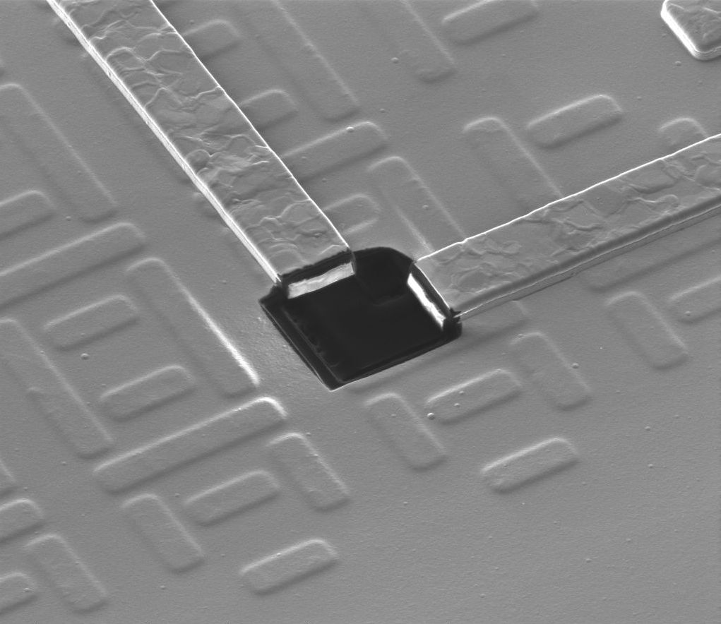
Circuit repair

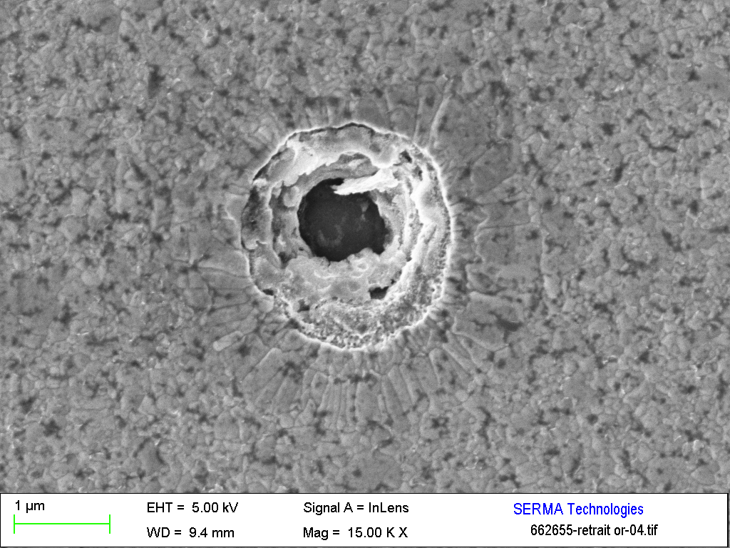
Metal line cut thanks to Focus Ion Beam. Details

Failed Capacitor

Short circuit observed into the insulator of a capacitor. AsGa technology. Details

FA ESD

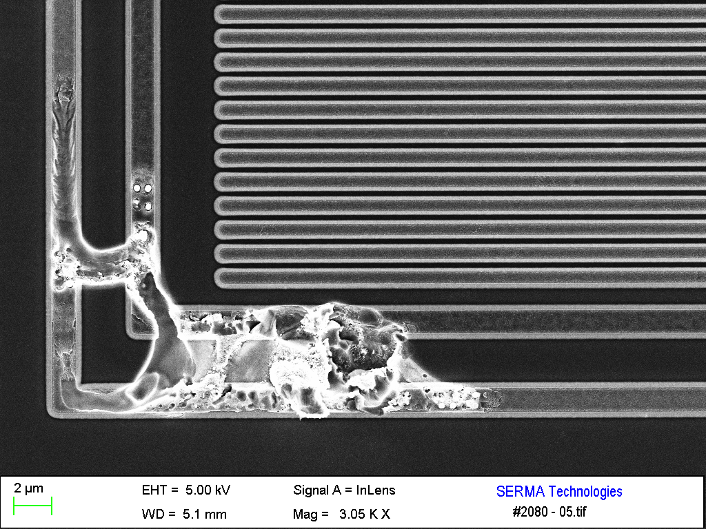
Failure into guardrings after ESD stress. Details

FA LIT

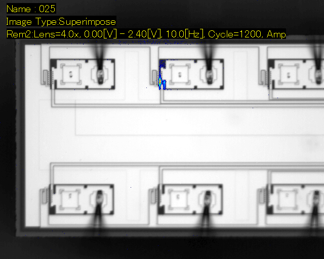
Lock in thermography of an electrical leakage. Details

TEM EDX

TEM EDX on magnetic sensors. Details

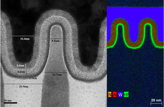
14nm FinFET

TEM construction analysis of a 14nm FinFET - SAMSUNG. Details

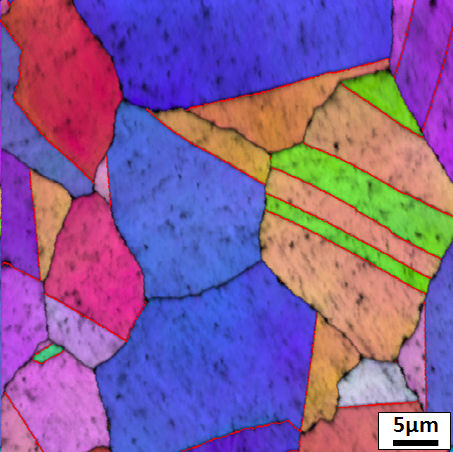
EBSD

EBSD maps from a NiCo film analysed by 3DSV technique. voxel size of 100 nm3. Details

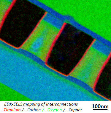
TEM EELS

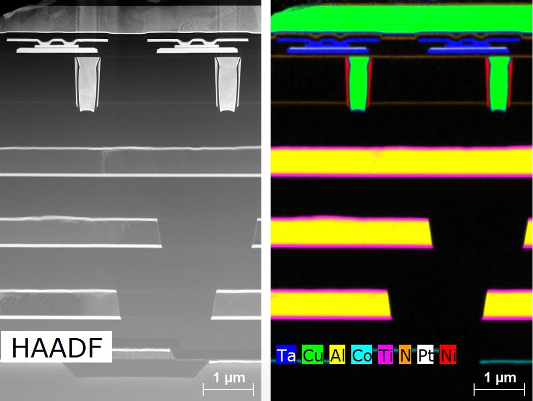
TEM Characterization of advanced interconnect system. Details
They trust in us ...

Contact

Get In Touch.

If you meet an issue in your development or you would like to request a service from our laboratory, you are invited to get in touch with us by filling up this short form. Someone from our team will kindly answer to your demand

Send Us A Message
Sending...
Your message was sent, thank you!
Contact Information
Where to Find Us

SERMA Technologies
MINATECH - BHT - Bat52
7 Parvis Louis Néel, CS20050
38040 Grenoble Cedex 9, FRANCE

Email Us At

p.salome@serma.com
admin-g@serma.com

Call Us At

Phone: (+33) 4 38 02 36 80
Mobile: (+33) 6 80 99 25 15
Fax: (+33) 4 76 96 25 40